With the first revision of the 68komputer boards and the required parts finally in hand, I spent the holidays (inside, in the warmth) assembling one. While it didn’t completely work, it also wasn’t a complete exercise in futility and a waste of time.
If you came here looking for a fun happy story of 68k code working, sadly this is not (yet) it. There were a few rather glaring flaws in the CPU board that precluded it from working much further than validating the mechanical design, GAL logic and a few of the peripherals; most of these issues are documented here. This post is mostly a bunch of pretty pictures of the stuff that does work, or just looks neat.
Test Fixture
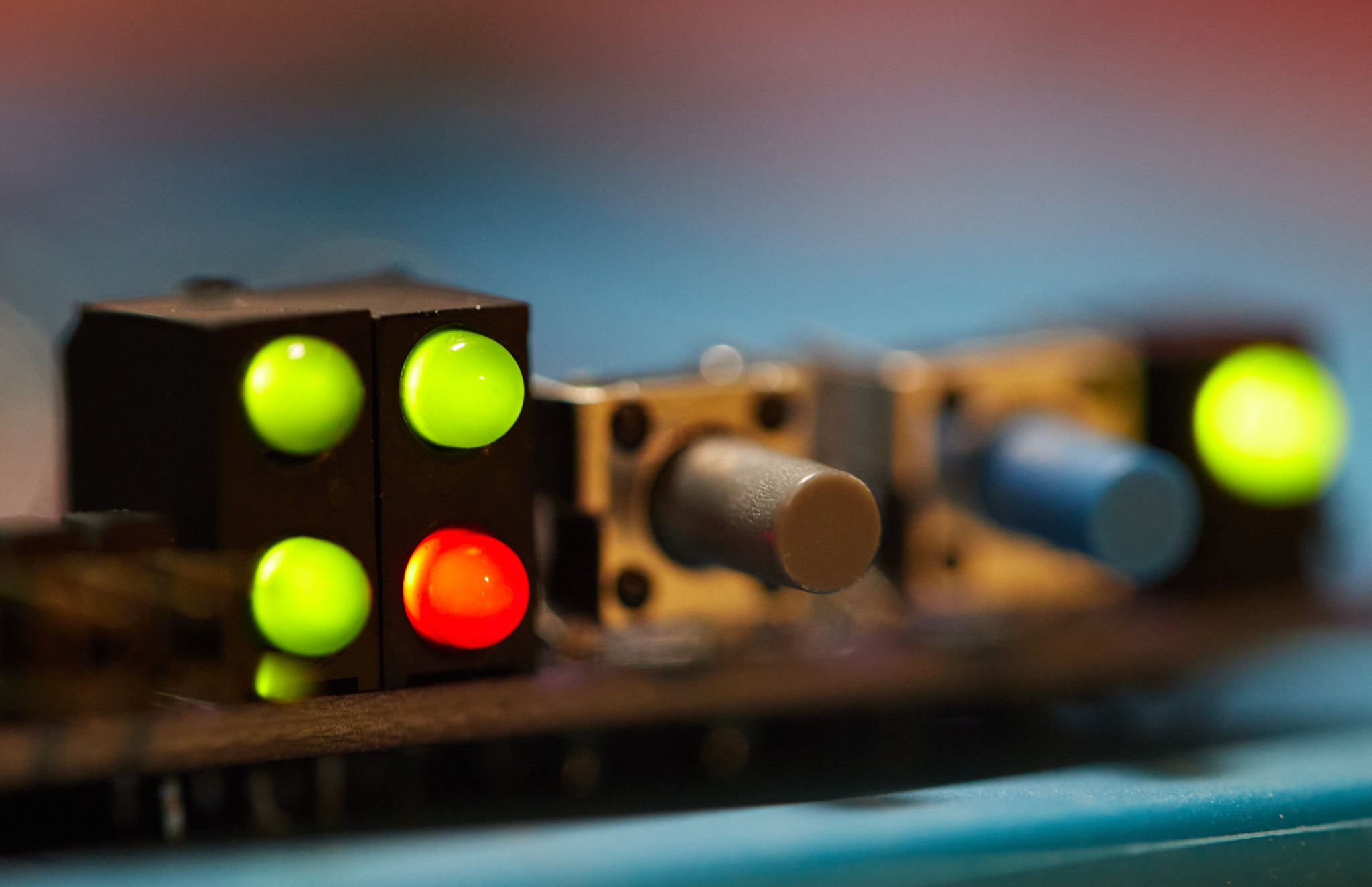
This was the first board I started assembling and comparatively speaking, I had next to no problems assembling it, or with the actual functionality of the board. In summary, this is just a little test fixture for the 68komputer; it consists of a Teensy 4.0, a metric shitton of IO expanders connected to every single bus IO line, a 5V power supply, and a couple blinkenlights. It also has some pin headers for hooking up a logic analyzer: much more convenient than trying to probe on the CPU board itself.
![]()
Initially, this board was going to have some sort of ARM chip of its own on it, instead of the Teensy, with plenty of IOs to directly write to the bus, rather than requiring a bunch of expanders. However, trying to get an STM32 or other microcontroller right now might as well be impossible. I hadn’t worked with the Teensy before, and while it’s certainly overkill for this application, it worked extremely well. I’m sure I’ll be revisiting the Teensy with future projects.
This board is basically fully functional – aside from a few stupids, such as the incorrect buffer for the reset/halt LEDs (they are inverted) and incorrect pinout for the logic probe connectors, neither of which affect the primary function – which was a very pleasant surprise.
Power
Besides providing control over the 68k bus, the secondary purpose of the test board is to provide power to the CPU board plugged in. Currently, the backplane pinout specifies +5V and +12V power. The debug board is set up to have an input for +12V, which is regulated to generate 5V onboard.
It’s based around the Rohm BD9C301FJ which is a pretty bog-standard synchronous buck converter – and one of the few that was in stock at Mouser at the start of December when I designed this board. It’s capable of providing up to 3A of current, perfect for driving some LEDs, the Teensy and CPU board itself.

I copied the schematic verbatim out of the datasheet but ended up going a little different route with the layout. I haven’t done any analysis whatsoever on the output of this supply, other than that it doesn’t look too shitty on my scope, and that stuff works when powered from it, so it probably doesn’t really matter here; it’s a nice 4 layer board with a solid ground plane, anyways1.
At some point I got a couple of TIL311 smart hexadecimal displays to show the values on the address/data bus as well, which also needed a source of 5V; this is drawn off the same regulator, through a dedicated polyfuse.
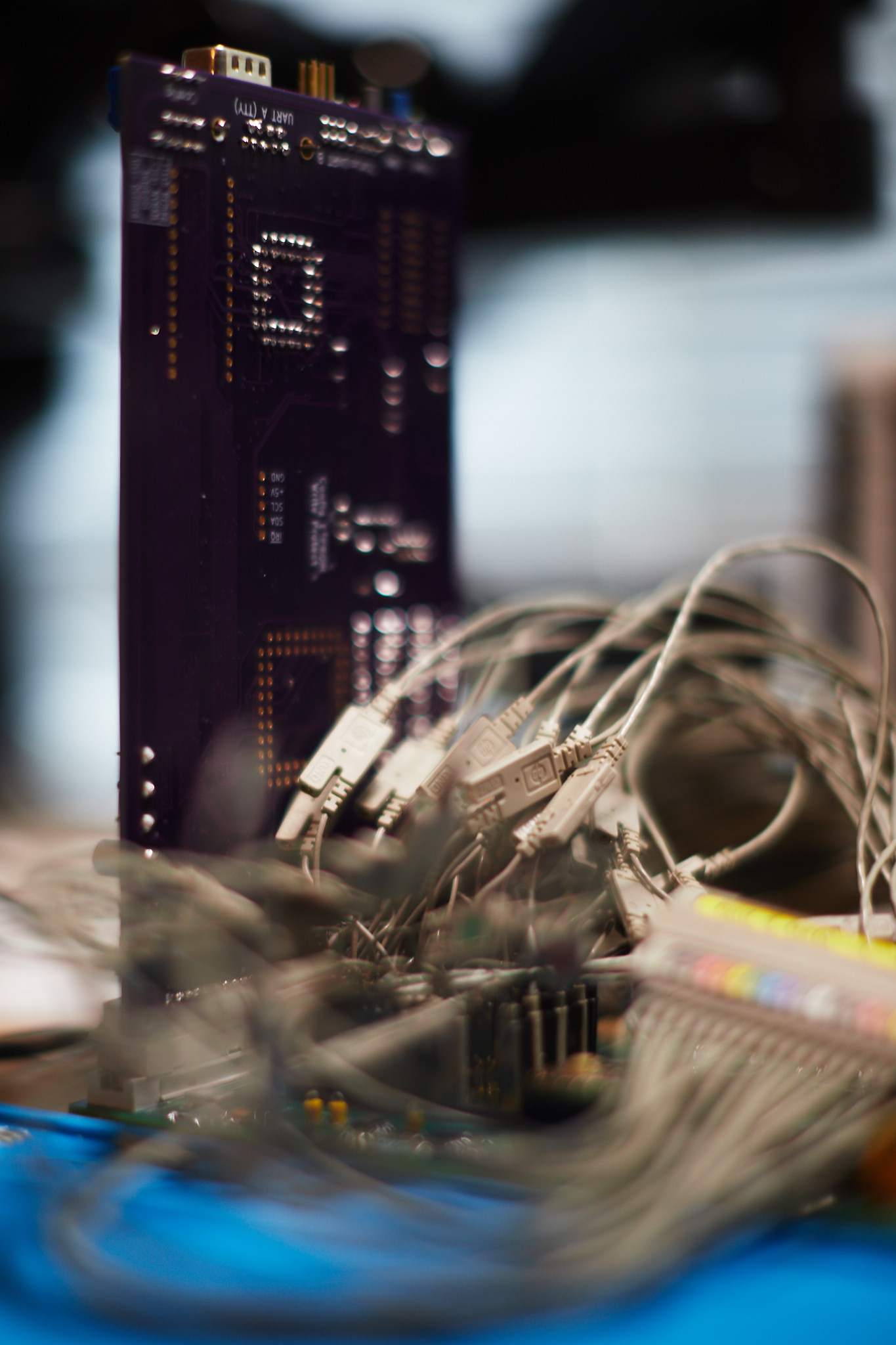
Bus Interface
Connecting up to the 68k bus requires quite a few IO lines: more than the Teensy has out of the box. Naturally, the fast SPI port lent itself to adding a bunch of IO expanders, so that the full address bus, data bus, and control lines can be controlled.
Including all of the overhead of the SPI transactions (at the maximum ~26MHz speed supported by the expanders) a single bus cycle can be done in roughly 800ns. This is of course a fair bit worse than the real 68000 would, but it should be sufficient for testing purposes.

There are a few extra bus lines (namely, those that control the pacing of bus transactions, such as /AS and /DTACK) that are connected directly to Teensy IOs via level shifters. The same goes for /RESET and /HALT so that single-stepping can, in theory, be implemented in software, but I haven’t bothered with that yet.
Since the Teensy is a 3.3V device, these expanders also are 3.3V. To simplify the design, I selected the XRA1403 expanders, which have 5V tolerant inputs. Since they’re powered from 3.3V, however, \(V_{OH} \approx 2.8V\) which is sufficient to switch TTL logic on the CPU board.
CPU Board
Now, on to the CPU board, arguably the star of the show. This is where things started to go downhill. It started with innocuous issues, like the reset buttons being inverted (no big deal – a simple rework is all that’s needed) and quickly snowballed from there.
I got fairly far through the assembly process before I realized I ordered the wrong footprint for a component, which meant waiting another few days for all of Mouser’s stock (all 8 of them…) of that chip to show up, in the correct package. Only once I soldered all those did I realize that I screwed up the control lines for the buffers, which meant the GALs couldn’t decode the bus state and drive the bus directions right.
What this means is that the expansion slot would never work, and bus mastering also would not work. If I could’ve programmed the flash chips before soldering them, the board likely would have worked, but this way it would end up being little more than soldering practice. Whoops…
Rev 2
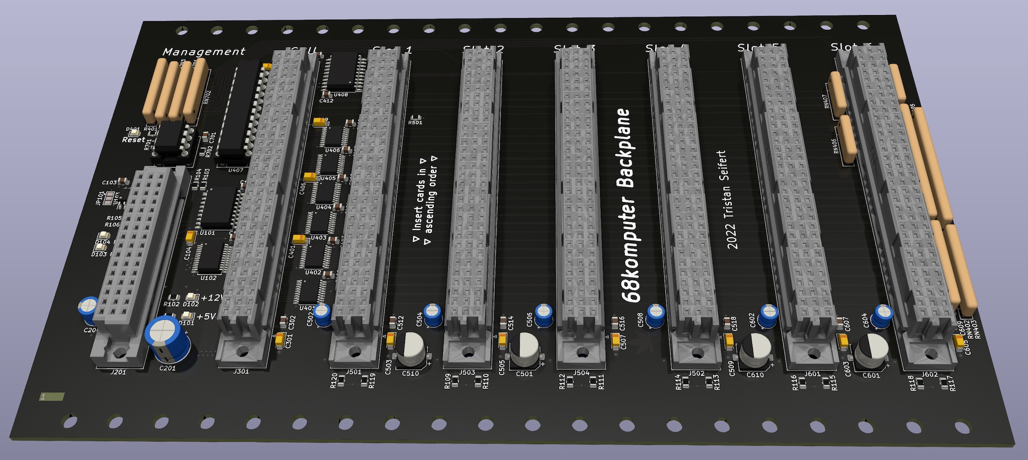
For the second revision, I dropped the bus buffers (they are now on the backplane,) which gave me back enough space to replace the surface mount flash chips with DIP sockets, so I can avoid having to program them through the test fixture to begin with.
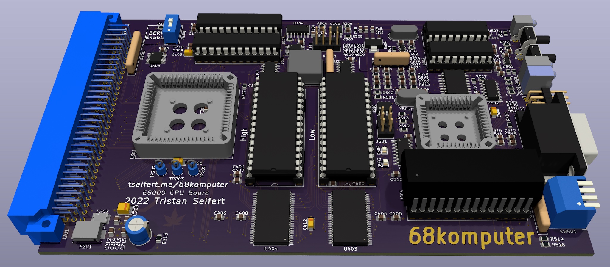
Other than that, most of the board is otherwise unchanged, aside from a few minor tweaks to footprints and component spacing to simplify assembly. There were also a few incorrect footprints that I ended up fixing, as well as adding some additional signals to the backplane connector.
Conclusion
It’s a little sad that the CPU board didn’t actually work this first time around, although it was nevertheless a good test for all the pretty little components I selected, and confirmed that the footprints I drew up and mechanical/3D models are reasonably close to reality.
Of course, as I write this, I’ve basically already wrapped up laying out rev 2 of the board, along with a few other goodies I didn’t have finished by the time I ordered the first revision boards, such as the backplane and a few peripheral boards – I’ll be writing about those soon.
Hopefully, I’ll get these updated boards checked out, and sent off to get manufactured sometime in the next week or two. I’m trying to write stuff more frequently here, and after all, I didn’t suffer through hours of recompiling toolchains only to not run my fancy new boot ROM on real hardware.
Apparently, switching supplies are super complicated and nobody really understands them, which is why layout recommendations are a thing. ↩