Most of the parts for the 68komputer have been ordered. Now the wait begins!
I realized I had a (basically complete) design for a 68008-based SBC kicking around my machine, so I decided to spend a weekend doing a totally normal thing of having a few drinks and routing a circuit board – if nothing else, as an excuse to use the 16702B Logic Analyzer I got my hands on recently.
Background
I’ve dreamt of building a 68000-based machine of my own design for quite some time. My first exposure to the 68k was the Sega Genesis/Mega Drive – specifically, making ROM hacks of the classic Sonic games. I spent a few years doing a good bit of research on that platform, but always wondered – what could I do with some more “modern” tech, a 68000, and enough self-hated to voluntarily write big chunks of assembly?
After a bit of research, I settled on using the 68008 (which is a 68000, but with an 8-bit data bus, and a narrower address bus) for this machine, mostly because the smaller bus width simplified board layout significantly. Plus, this way I can be lazy and won’t have to burn both a high and a low byte ROM, heh.
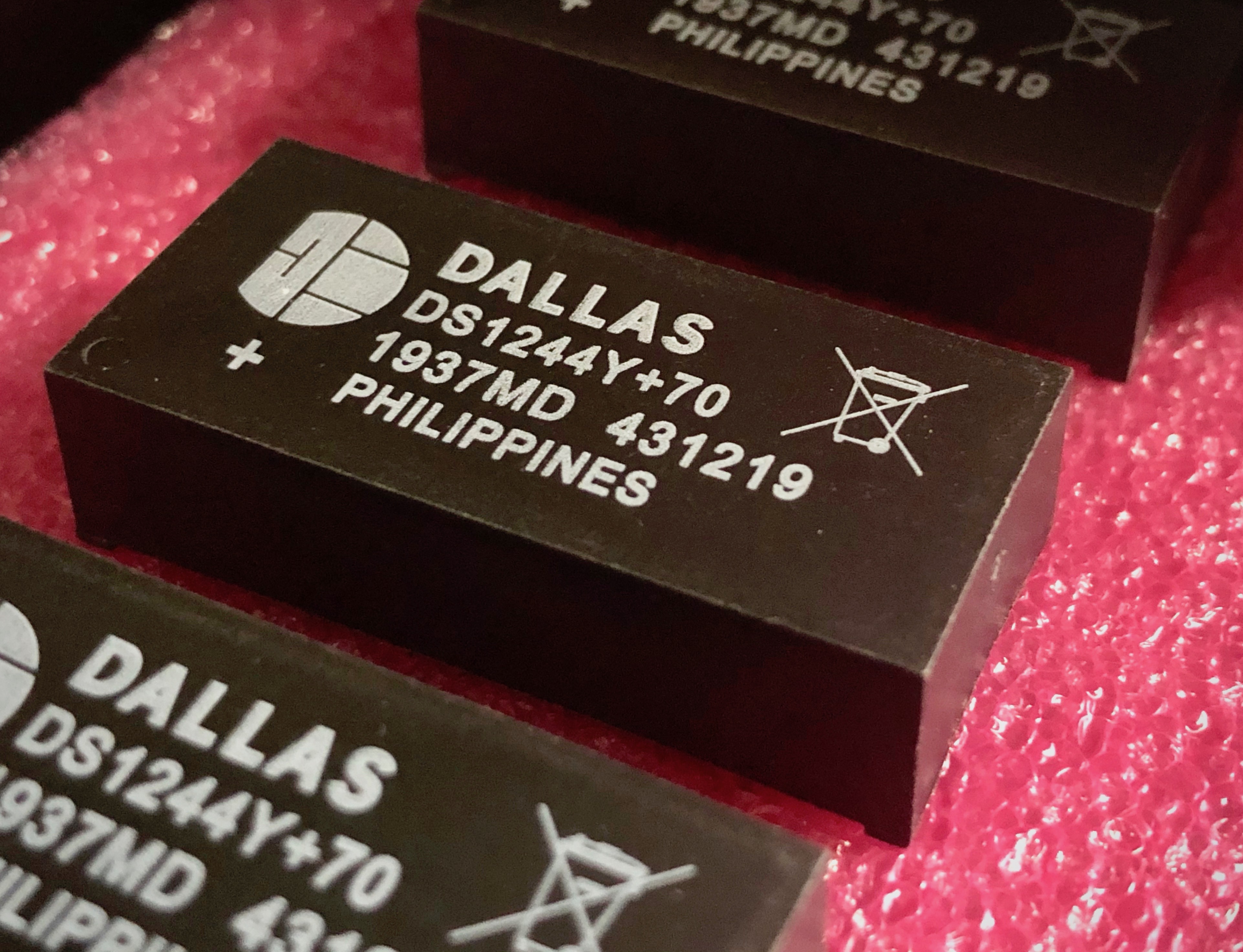
Thus, the 68komputer was born – a rather bare-bones 68k-based SBC. On board are 512K of static RAM, a 128K flash ROM, an DS1244, which is a 32K NVRAM + RTC combination device, and an XR68C681 – an improved version of the original Motorola 68681 – to provide two serial ports, a 16-bit timer/counter, and a set of input/output ports. Two of those output pins are connected to LEDs on the board… because what computer wouldn’t have blinkenlights?
Eventually, I plan to build a version of this machine with a full 68000, which will hopefully be (mostly) software compatible, and allow me to map more than just a “measly” 512K of RAM. At some point, I’m hoping to be able to find a good, reliable source of 68030 chips and build a machine around one of those, but that’s probably a project for when I’m not a broke college student.
Hardware
As far as the hardware goes, this design really is nothing special, and is pretty similar to most bare-bones 68000 computer designs. I opted to use mostly through-hole ICs to keep the aesthetic of that mid-80s computer design; however, I opted to use GALs (specifically, the GAL22V10) rather than a bunch of discrete logic, and use surface mount capacitors/resistors for space reasons.
Every IC is socketed, which should make testing and debugging relatively simple. I’m thinking I can probably fit a ZIF socket for the boot ROM as well, which will make debugging flash writing routines a lot less painful, heh.
Schematic
I tried to do my best to keep the schematic simple and easy to follow, but there really isn’t a whole lot to this machine – this’ll hopefully make debugging easier later, but “famous last words” and all that.
The full schematic in EAGLE format is available on my GitHub repo for this project. The board layout is in that repo too, along with a library of parts I’ve used/tried to use for this project.
CPU, RAM, ROM
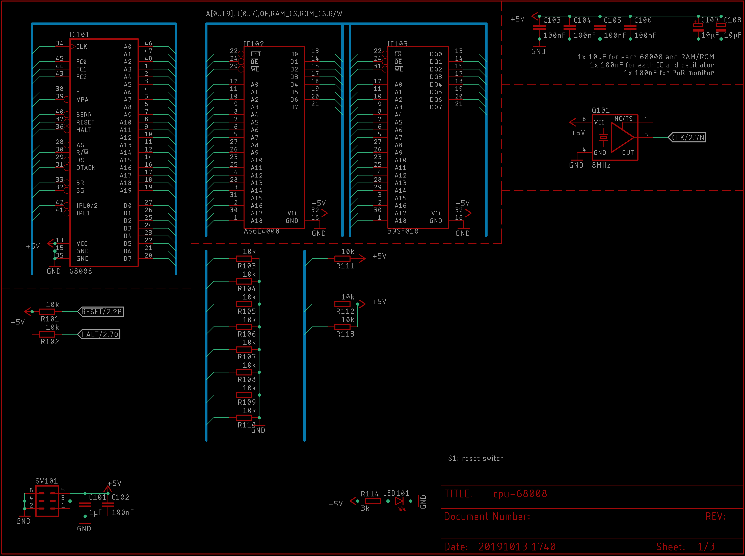
This part of the schematic contains the 68008 CPU, the 512K of static RAM (an Alliance AS6C4008), the 128K boot ROM (a SST39SF010, though any chip with compatible pinouts will do), and an 8MHz TXCO. There’s also a couple of resistors to pull various lines (the data bus is pulled to ground, BR, VPA, and BERR are pulled high) to well defined state, especially while the CPU is in reset.
We also have a little set of pin headers to input 5V power to the board, as well as the obligatory power LED. You’ll probably also notice the pile of decoupling in the top right of the schematic: I tried to have a 100nF cap for every chip, and a larger 10µF cap near most major areas of the board.
Peripherals
Obviously, this system isn’t much good without a way to connect to the rest of the world.
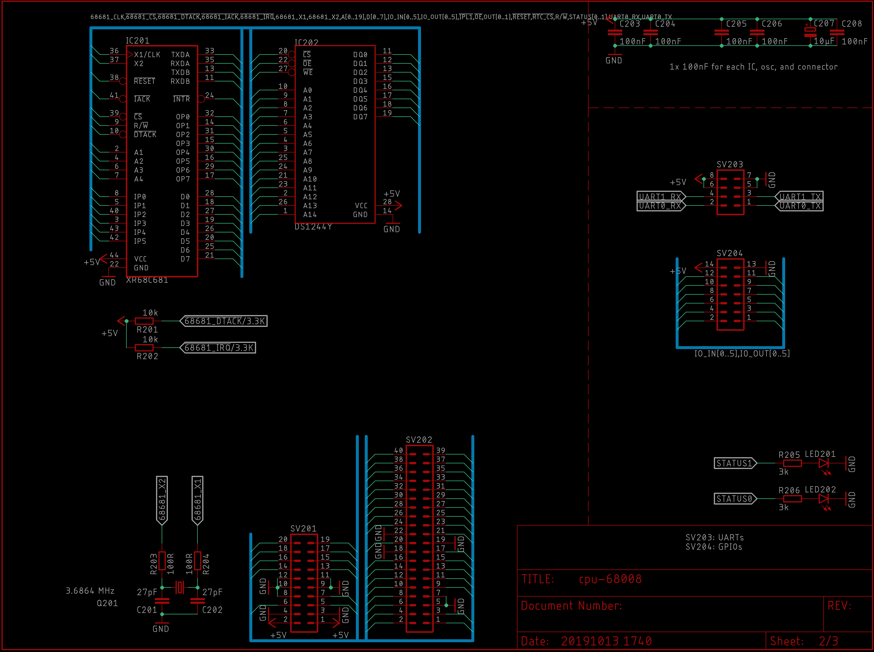
Next up are the system peripherals. This would be the XC68C681 (a 68681 DUART derivative) and the DS1244 NVRAM/RTC. Both serial ports, and most of the input/output lines from the 68681 are broken out to individual headers, with two output bits connected instead to a set of LEDs. The DUART gets its own crystal (a nice, even 3.6864 MHz, anyways) for baud rate generation.
Originally, I had a TXCO at that frequency that served as the clock for the DUART and rest of the system, but the 68008’s I have will run at up to 10MHz, and I’ll take every bit of speed I can get, with this being a 32-bit CPU constrained to an 8-bit data bus.
We also have the 60 pin header (okay, I cheated, it’s a 40 and a 20 pin header smushed together… sue me) that’ll serve as an external bus interface. It’s got the entire set of 68000 bus control signals, the full address/data bus, the system’s 8MHz clock, chip select for the bus area, and a mechanism to trigger an interrupt.
Glue Logic
Lastly, we need some glue logic to tie this whole thing together. Some people prefer to use 74-series logic for this, but I opted to use GALs to conserve board space, as well as my sanity. I originally planned to use a CPLD, but couldn’t track a 5V-compatible one down.
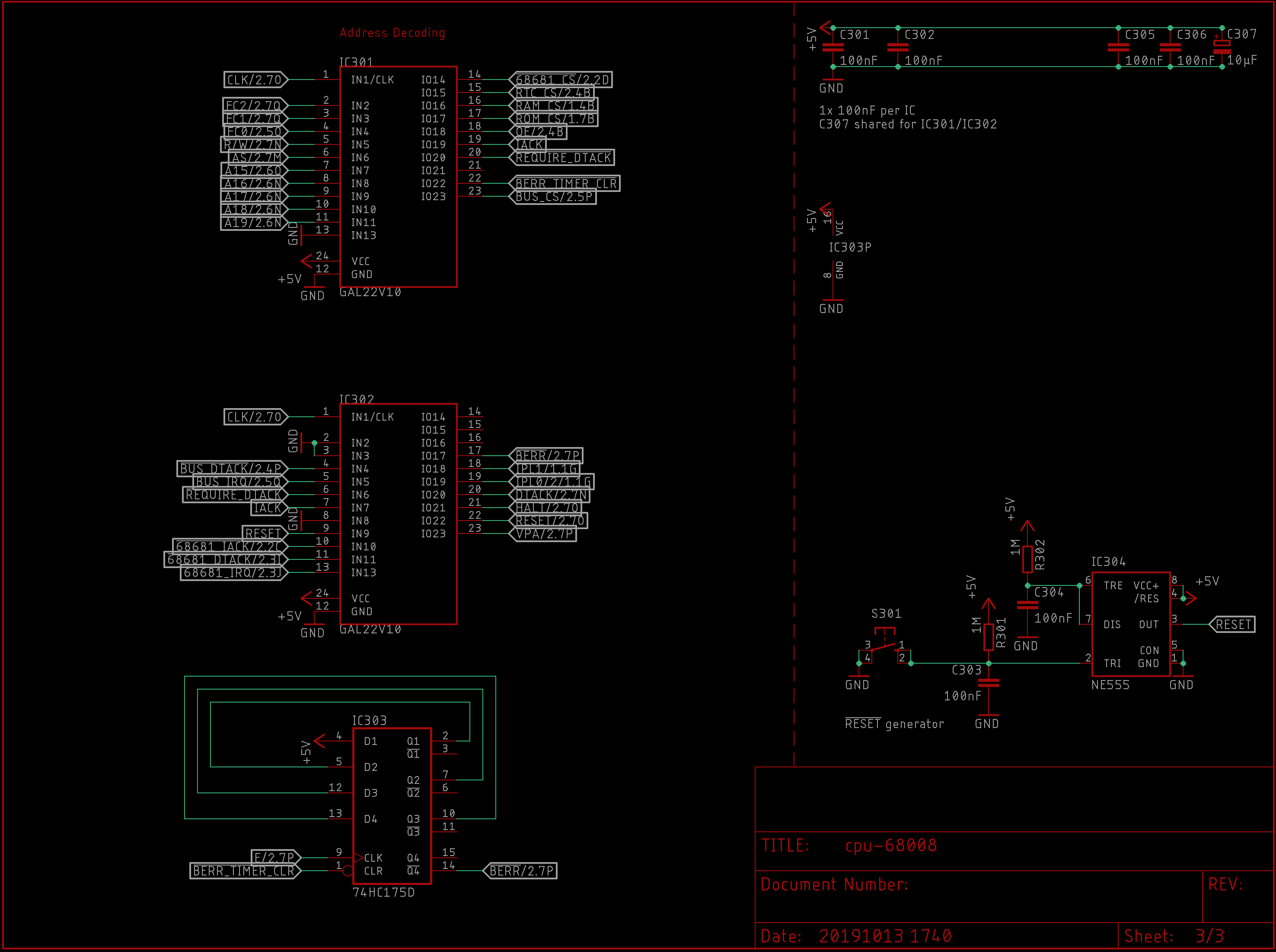
Aside from two GAL22V10’s, there’s also a classic 555 timer to generate both a power-on reset, and to debounce the reset switch. The output of the timer feeds into the GALs, which then in turn will assert both RESET and HALT simultaneously.
There’s also a ‘175 flip-flop, clocked by the CPU’s E output, which runs at 1/10th of the CPU clock. This works as a timer to generate a bus error if no device asserts DTACK within 4 E clock cycles, and should help keep the system from locking up when programs go haywire.
Boards
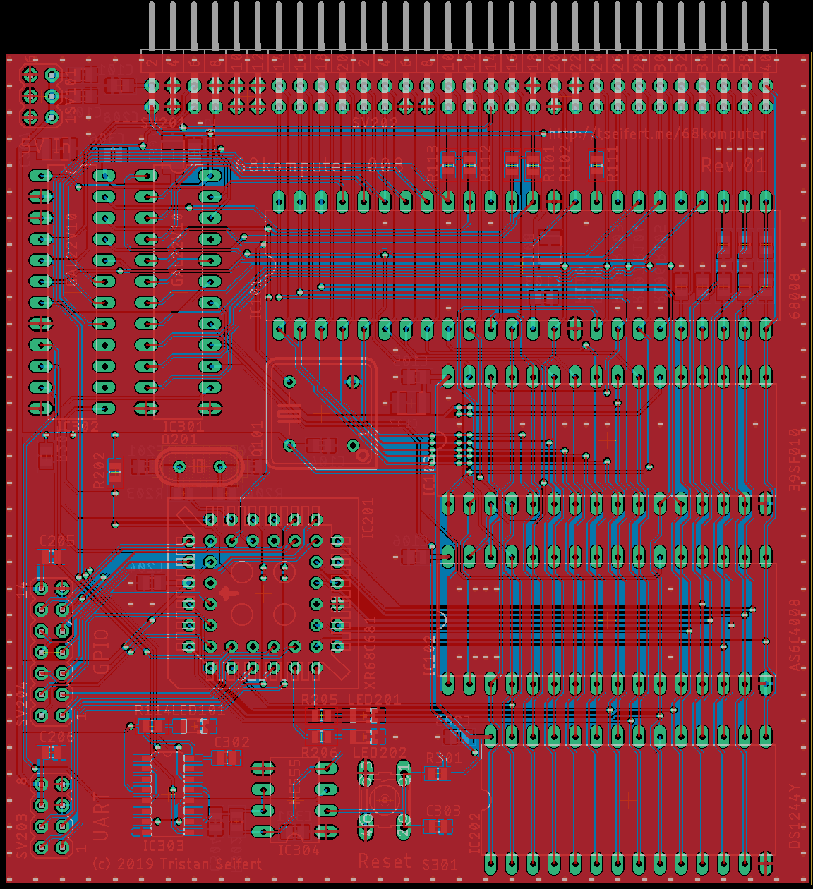
The circuit boards were ordered from DirtyPCBs and should be arriving any day. Most of the electronics are coming from Mouser hopefully this weekend, with a few other odds and ends I either already have on hand (68008, GALs, oscillators, etc.) or have requested as samples.
Until then, here’s an up close look at the routed board – which, in typical fashion, contains a mistake (forgot to connect DS to the GALs) I didn’t notice until immediately after I sent the boards off to manufacturing… meh! Worst case I’ll have to add a bodge wire, but I think I can work around this issue.
Expansion
You probably noticed the big 60-pin connector at the top of the board. That carries all of the 68008’s control signals, the full address and data bus, as well as a few additional lines for address decoding and interrupt generation by external peripherals. My plan is to eventually design a board that connects to it, and acts as a sort of backplane for different peripheral boards.
There’s a few peripherals I’m going to start off with – the first being a sound card based around the YM3812 (OPL2) and YM2149 (A clone of the AY-3-8910) chips, both of which I picked up at a vending machine on one of several visits to Akihabara during my Japan trip this summer. I also have the classic TMS9918 video chip that would be cool to use, especially since this chip is a distant ancestor of the Mega Drive VDP that I love to hate so much. (This obviously means I’ll have to write some neat demos for this thing…)
Later on I’d like to implement some sort of permanent storage (probably an IDE interface, which would let me use CF cards pretty easily) that more complex programs can be loaded from. Some sort of additional serial interface card would also be convenient for having this thing talk to the outside world: applications like turning this thing into a MIDI synthesizer come to mind.
Ideally, I’ll have this backplane designed in such a way that adding a wider address and data bus for the full 68000, won’t be too terrible, and I’m sure I can take some cues from how the ISA bus solved that same problem, but it probably is going to boil down to address decoding. The 68k has the lovely MOVEP instruction that makes dealing with 8-bit devices on a 16-bit bus super easy without much performance loss.
More pretty pictures
Here’s a glory shot of the DS1244 NVRAM/RTC combo. These devices are pretty cool, because they have a TXCO and Lithium battery built in to the plastic DIP module – as far as your system is concerned, it looks exactly like plain old SRAM. Accessing the clock part of the device is a little weird (it’s done through a 64-bit “recognition sequence” written to D0) but that’s code I’ll have to write exactly once, throw in ROM, and never touch again.
All the other parts, including the boards, are still in the mail. Knowing how absolutely god-awful College Station’s post office is at actually doing their job and delivering packages, it’s entirely possible I’ll be waiting more than just a week, but I’m looking forward to putting this all together.
Software
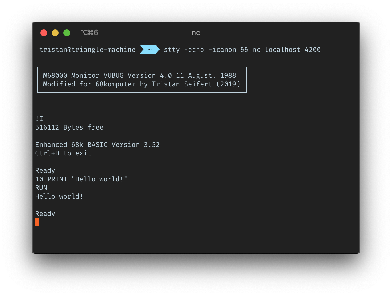
In the time between ordering parts and waiting for everything to arrive, I’ve started working on the Boot ROM for the machine. This ROM contains a monitor – version 4.0 of VUBug, a relatively fully featured 68k monitor written at Vanderbilt University. This provides a basic environment that the system can boot into, and allows uploading of programs through the second serial port of the hardware. Additionally, it features facilities to dump and modify memory, and produce a disassembly listing of memory, which is a pretty cool feature. It also offers trace/single stepping, and rudimentary breakpoint support.
Since no wanna-be retro computer is complete without a BASIC interpreter, I’ve also ported Lee Davison’s Enhanced Basic (version 3.52) for 68k to this machine. Davison’s website has been down for quite a while, but I was able to find a mirror of the sources to the interpreter on GitHub and ported them pretty easily: all you need to provide to use the interpreter are some routines for character IO, and optional load/save routines, which are unimplemented for now.
Because I don’t have the physical hardware to run this on (and even if I did, flashing a ROM every time I make a tiny change would be a massive pain in the ass) I developed a little quick and dirty emulator. Only ROM/RAM and the DUART are emulated – and even then, only serial IO is implemented, with no support for timers – but that’s good enough for testing the monitor. The core of this emulator is based around the Musashi 68k core with a bit of glue logic to handle address decoding and other such fun things.
I may end up putting the source to that emulator on the GitHub repository with the rest of the Boot ROM, but it’s probably some of the worst code I’ve ever written and amounts to nothing more than a disgusting hack, so meh.
Down the line, the plan is to give the boot ROM some more “substance” – e.g. abstracting things like disk IO into traps, which expansion hardware could hook into with drivers in card space. This will probably require the full 68000 for its larger address bus to make peripheral option ROMs realistic.