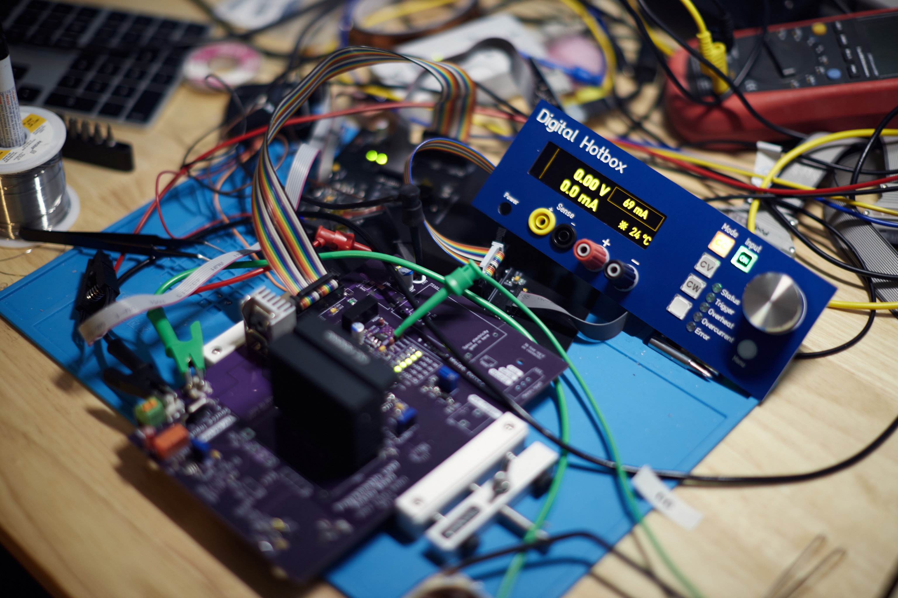
After a much-needed vacation, I’m back to working on my programmable load. Time to remember what parts worked and which didn’t for the inevitable ∞th revision.
Update: There’s even more! Check out the follow-up post to see what I do best – overengineering seemingly simple projects.
Stuff that worked
Most of the software on the controller side worked, which I knew from previous tests on the hardware I described in a previous post. Since then, I’ve gotten the USB stack working, including writing some basic host-side tools to communicate with the device and read out some information.
There have also been improvements to the quality of the codebase, and bug fixes in drivers across the board. A few hardware components are worth calling out specifically, though:
Front Panel
The front panel was probably the closest component that was 100% functional. Aside from some very minor rework (namely, enlarging the hole for the menu button about 0.2mm with a file) everything fits properly and looks really surprisingly good, too.

I had the front panel manufactured by Front Panel Express, which is located right outside Seattle. That means they showed up extremely quickly, once the design is submitted on their website. Front panels are designed with their custom CAD software (which certainly does the job) which has the benefit of providing a very detailed pricing breakdown for every step.
Also, they include candy with your order. That alone is enough to earn my business.
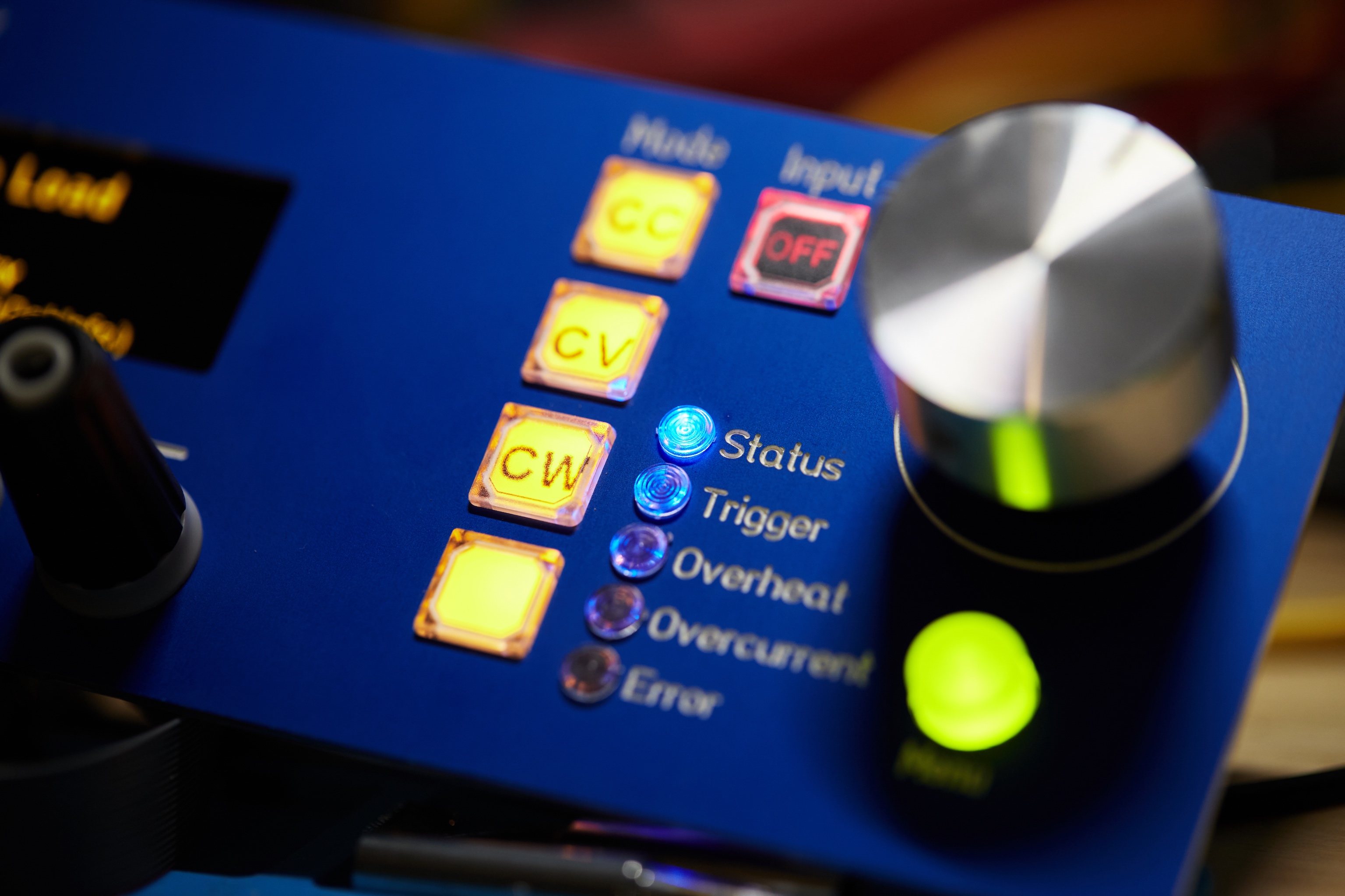
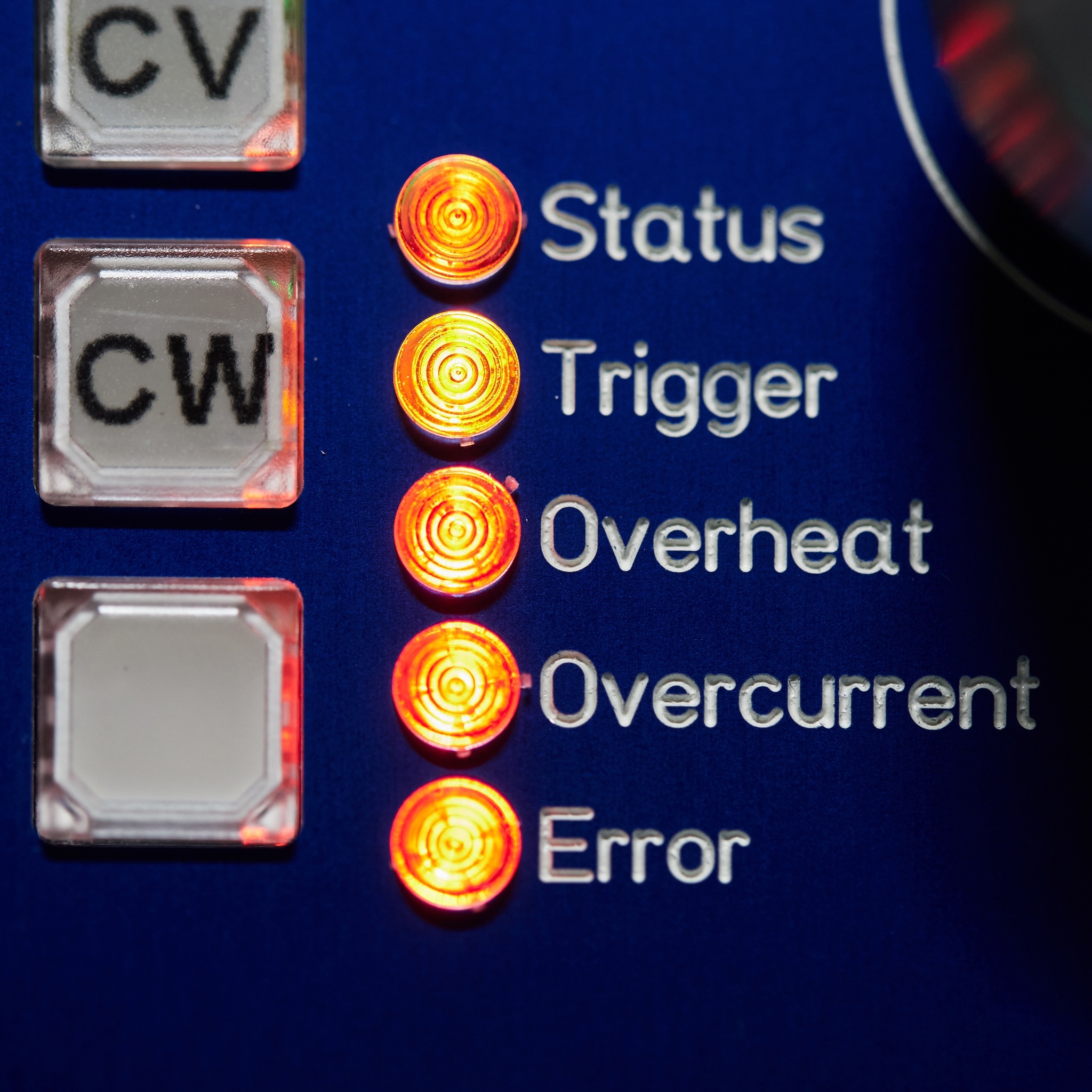
Button Board
This is the largest board on the front panel, which holds all of the buttons, indicators, and the rotary encoder. It’s nothing more than a LED driver and IO expander, both connected via I²C to the host.
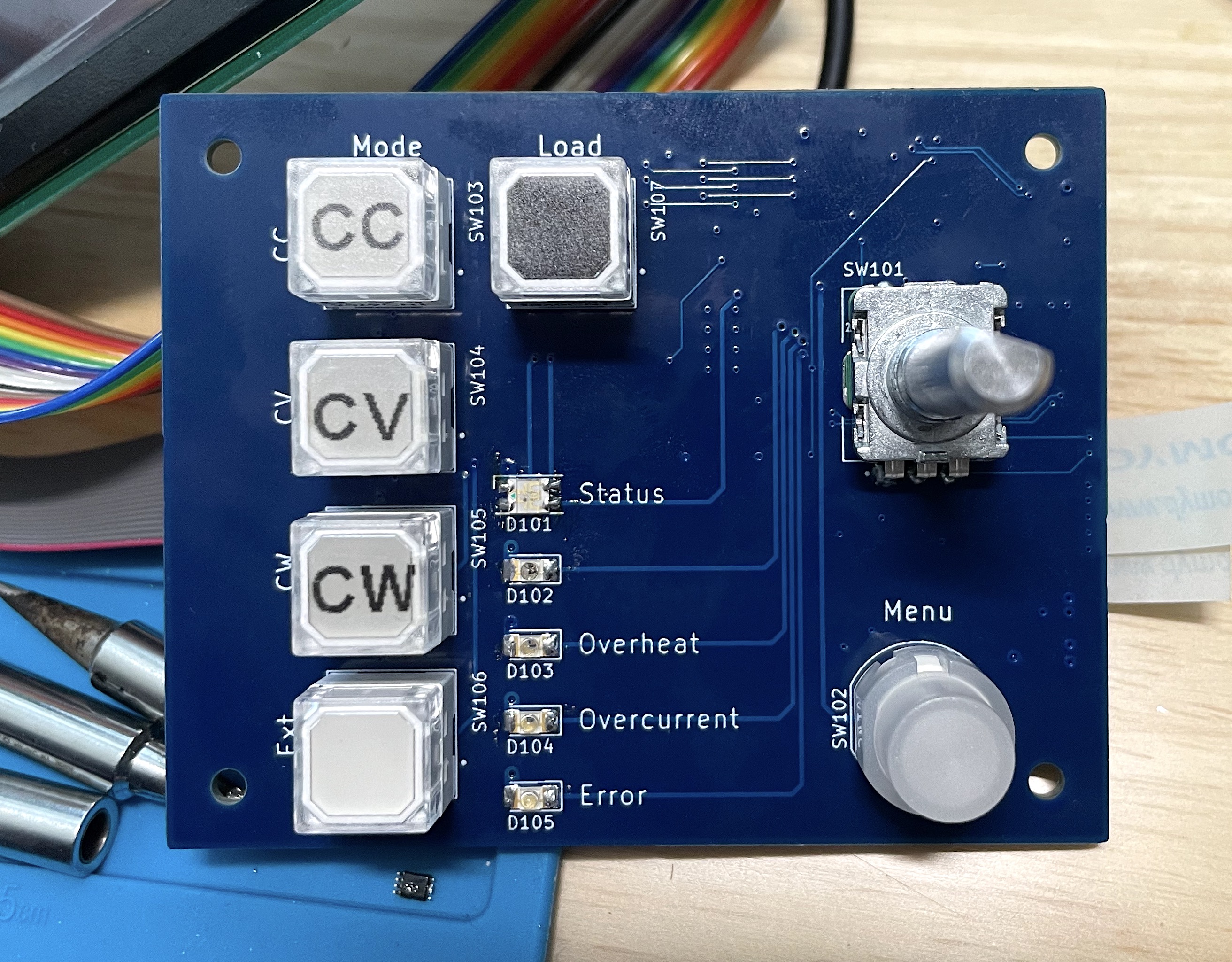
It’s mounted to the back of the front panel on dedicated M2.5 standoffs (which are attached firmly to the front panel during manufacture) which conveniently keeps it at a well-defined distance from the cutouts on the front.
As far as buttons go, the rectangular illuminated “ice cube” tactile switches are Omron B3W-9 which are available in a large variety of single and dual illumination colors. The caps can be removed, so you can put a film containing a button legend inside. Here, I used a bog standard label maker to print my own labels, but also got a special film (supplied by Omron) that shows the ON/OFF label, depending on whether the button is illuminated red or green.
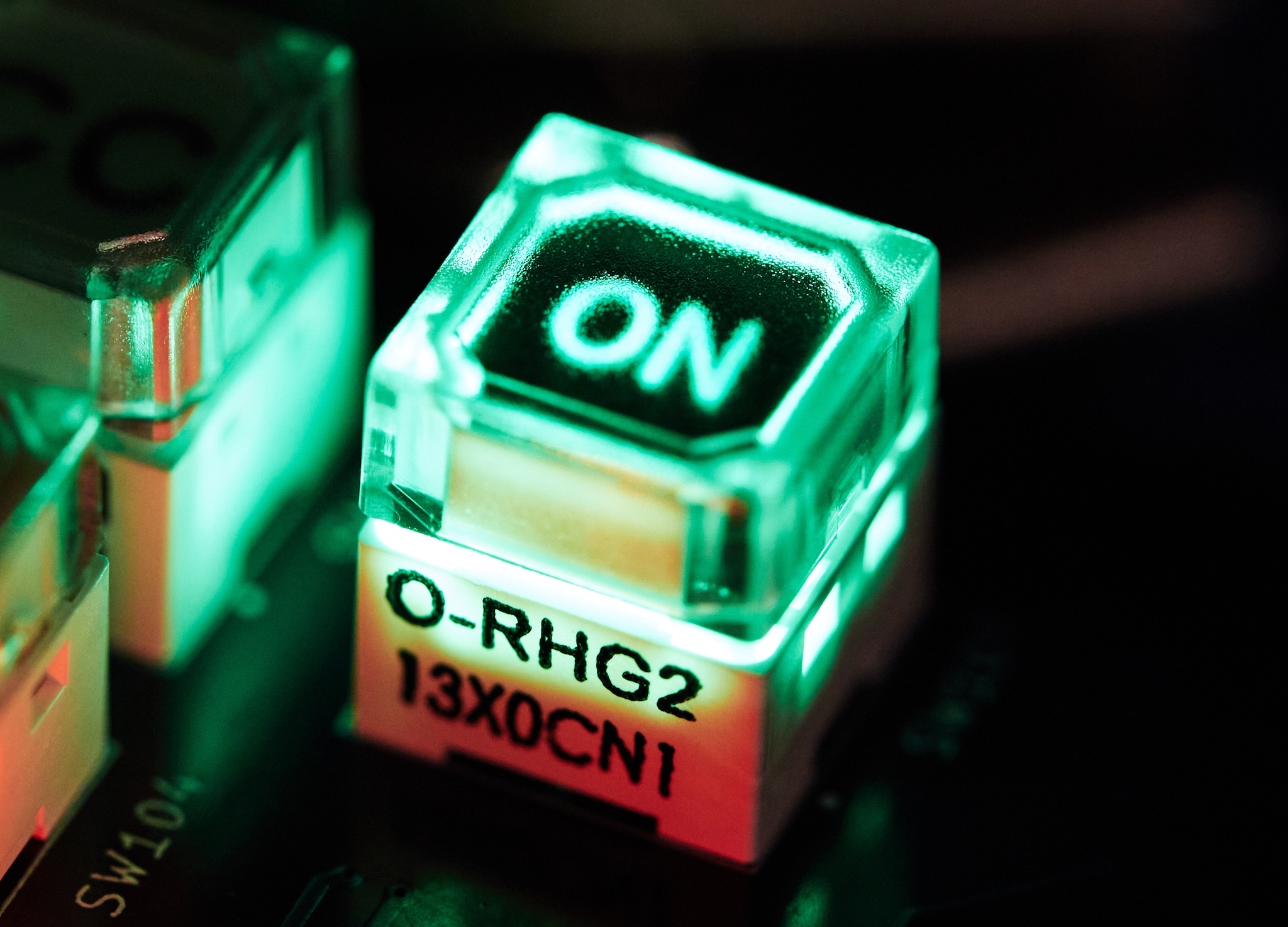
There’s also the menu button, which is one of the C&K D6 series illuminated tactile switches. Unfortunately, this one is a few mm taller than the Omron switches, so it sticks out a good bit more from the front panel – but this is probably a good thing for the “menu” button.
Lastly, there’s a bunch of LEDs (which are the reverse mount type but mounted the “right” way around – this was the cheapest way I was able to find LEDs with a relatively narrow beam angle) which are brought out to the front of the board by a few light pipes. These just press-fit (with a fair bit of force) into holes drilled in the front panel with a particular diameter. There’s still some bleeding through between adjacent LEDs, so I’ll probably have to come up with some (perhaps 3D printed) solution to block light between the pipes.
Analog Stuff
A fair bit of analog stuff ended up working after I corrected a few screw-ups to do with power supplies for op-amps with a second revision of the board.
Power Supplies
Since there’s lots of analog stuff involved here, there are also lots of power supply rails. The entire analog board receives an isolated ~15V supply, which is regulated down to several different voltages:
- +12V Analog: Powers the MOSFET drive op-amps
- +5V Analog: Source for -5V converter, relays, voltage sense amplifier
- +3V3 Digital: Powers all digital circuitry, such as the analog side of ADCs and DACs.
- +3V3 Analog: Derived from +3V3 digital through ferrite bead filters. Powers the analog part of converters.
- -5V Analog: Negative bias voltage for MOSFET drive (via negative reference adjustment)
These all worked, and I think looked reasonably alright as far as noise goes:
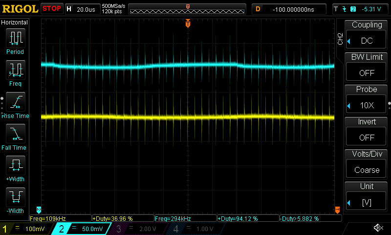
The ~100kHz switching frequency of the isolated +15V DC/DC converter (CUI PCN2-S12-S15-S) is clearly visible (Ch1, yellow) on the output; this is alright since nothing is directly powered from it. There’s also roughly 150mV of noise, which is again in spec for the device. The most important rail, +5V analog (Ch2, blue) is generated by a linear regulator off the +15V input. A bit of the noise is still coupled through, but it’s attenuated greatly (roughly 40mV peak-to-peak) and can probably be reduced even further with more filtering.
Voltage Sense
Input voltage sense actually worked flawlessly, which was expected, but still a welcome surprise.

A differential amp (A TI OPA277) is configured to provide a 50:1 gain so that the voltage read by the sense ADC will be \(V_{\text{sense}} = \frac{V_{\text{in}}}{50}\). The amp has high linearity, and RV501 allows trimming any remaining DC offset out of the system. Combined with high precision, low tempco gain resistors (R501-R504) I found that this provides excellent accuracy. D501 protects the converter from excess input voltages, and R505/C504 forms a low-pass filter restricting the signal bandwidth to roughly 1.5kHz.
The current design then feeds this into an I²C ADC (the MCP3421, which gives you results in 12 to 18-bit resolution, based on the sampling rate) that had an internal amp, so we can get a bit more dynamic range out of the ADC in low voltage ranges by amplifying the signal.
I had some issues with noise affecting the ADC, hence the addition of the common-mode choke L501 above. This is more critical as external sense inputs can have higher levels of common-mode noise.
Stuff that didn’t work
Most of the issues with the current state of the programmable load were either mechanical (e.g. boards with insufficient cutouts, incorrect footprints, etc.) or related to the analog board’s control loop.
Analog Board
The primary issue with the analog board wasn’t even that it didn’t work – it is possible to set a current (by dialing in the reference voltage with the current set DACs) and get reasonably close to it (though there are plenty of nonlinearities to be corrected) – but more so that the I²C bus used to control everything on the analog board is simply too slow. Even at the maximum ~400kHz supported by all components (specifically, the bus isolators set the upper limit here,) there’s nowhere near enough bandwidth to accomplish more than around 75 sample/update cycles per second.
While that doesn’t sound too problematic for just a constant current mode, it essentially makes implementing more complex operation modes impossible, since these modes would require a control loop in software to update the current setpoint much more frequently to be useful.
Another issue came from the current set DACs: I expected to be able to use their internal 2x gain, but this requires a supply voltage of at least 4V, or the part just goes into fault mode and outputs nothing at all. This meant that resolution in 1x mode wasn’t really that good, and the best I was able to accomplish was around 10mA.
Lastly, the ADCs were just too slow to really be useful. While they could operate at 18-bit resolution, this reduced their sample rate to less than 4 samples per second: basically useless. This meant the ADCs ran at 12-bit resolution, which even when coupled with aggressive adjustments of the input gain, did not yield particularly great accuracy. The current sense accuracy was only around 7.5mA, which is far worse than I wanted.
Compounding all of these troubles is that high I²C traffic is relatively CPU intensive, as there is no way to use DMA to help with many small bus transactions.
Going Forward
As you’ve probably gathered by now, I’m going to end up respinning these boards yet again, for yet another revision. I realized also now that I had more functional boards and front panels, and tried to assemble it all into the case I selected… that it’s insanely cramped. As in, “borderline impossible to assemble” cramped.
Since I already had the Technomet R110 in mind as a backup for the Hammond enclosure I went with, I knew that would have much more internal space for all the boards. This also has the added benefit that the controller board screws directly to the case, and the analog load board can easily be swapped out, as it will be mounted on card guides.
And to avoid the surprises of how things will fit together in the end, I finally got over my fear of 3D CAD software, and learned FreeCAD to throw a little something together, based on 3D models provided by Metcase (shown here with the top cover removed):
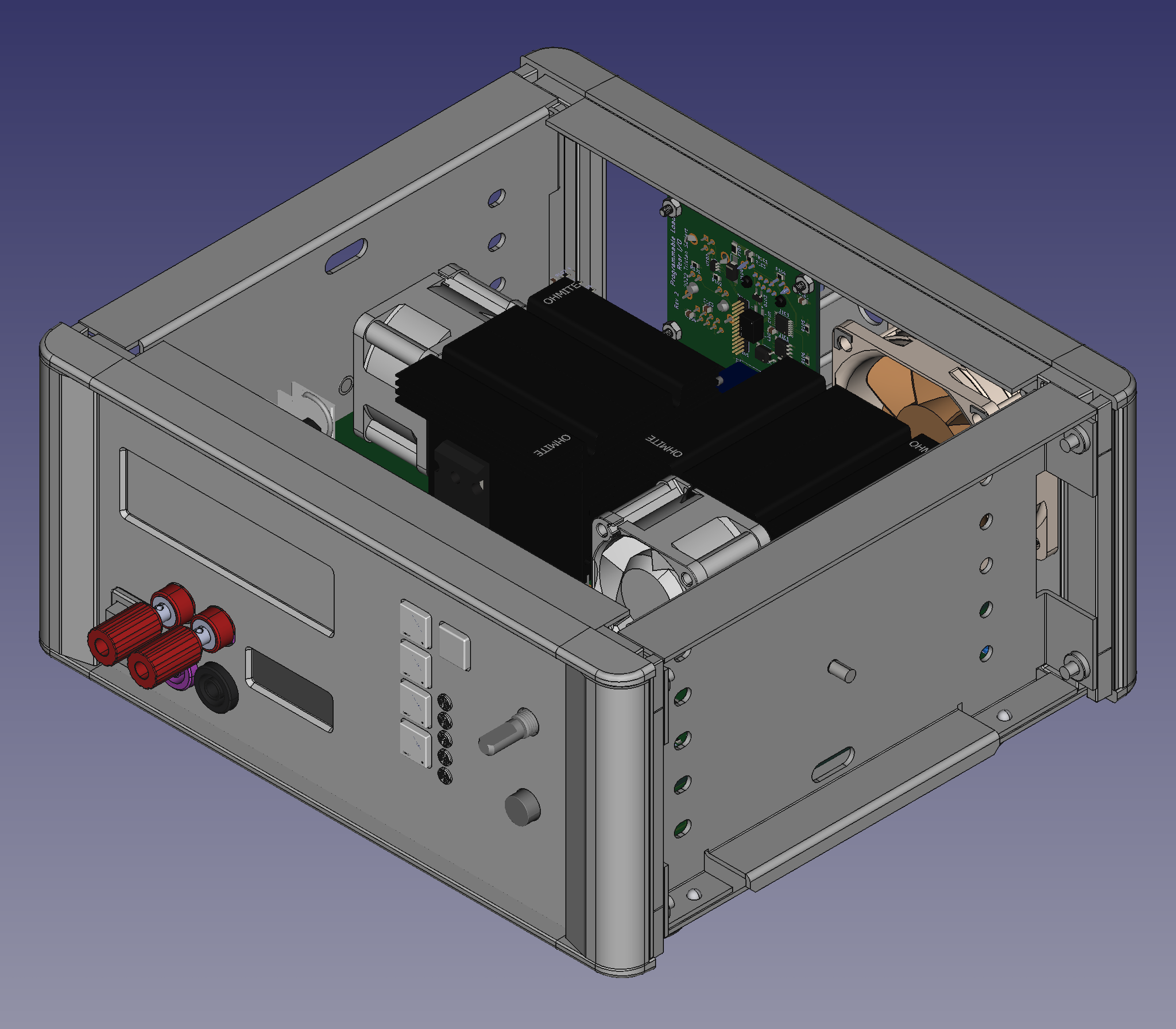
Additionally, I’ve been working on some board revisions to fit this case. The controller board now holds the mains power supply (which has been upgraded to a 30W supply) and handles input voltage sense. Additionally, the soft power switch is going away; in its place, there’s a proper hard power switch. More possibilities for future expansion are also present, in the form of a rear panel CAN bus, and a much higher speed SPI bus for internal analog board control.
I’ll also have to respin both the front and rear panels to fit this new case, which is a little annoying considering the cost; but this is also a good opportunity to improve the design (by adding some bevels, improving labels, etc.) a bit and (hopefully) learn to not make this mistake again 🫥
That’s it for now – hopefully I’ll have some more updates about this project in the coming weeks, since I should finally get around to finishing the new board revisions.