Faced with the prospect of another board revision and parts that became unobtanium, it was time to go back to the drawing board and figure out a way to use more readily available parts, while making the hardware more powerful and polished.
Update: There’s even more! Check out the follow-up post for details on the software stack involved.
I had a mostly working design with the previous revision but exhausted my stash of the ATSAME5x’s, and the earliest delivery dates from any suppliers were over a year out – so I couldn’t build any more if I wanted to spin the board to fix a few lingering issues.
Am I going to blame supply chain issues for this impromptu re-design? Yes. Have I had it in the back of my mind since I started this little side quest of a project in March? Also yes, but I’m not on trial here, so…
New Controller
Essentially all my issues with the existing hardware stemmed from design decisions made in the controller part of the project, rather than the analog side or user interface. Most of my attention in this redesign thus went to addressing these issues.1
The main issue I kept hitting very early on in the firmware development process with the original hardware (based around a ~120MHz Cortex M4F) was that there were simply not enough CPU cycles to go around to render the UI as pretty and responsive as I wanted to, while also maintaining adequate responsiveness over USB, all while minimizing jitter on the load’s input. And don’t even think about adding Ethernet to the mix!
Possible Solutions
This is a relatively common problem with realtime systems like this: separating the less critical components from the hard realtime tasks and trying to do so as cheaply as possible. This often leads to some “creative” software solutions or duplicated hardware in the form of two separate processors.
Here I toyed with a few different options, all of which centered around the common theme of a more powerful applications processor/compute module (I considered the Raspberry Pi, as well as the Onion Omega2 since I’d worked with both before) and some sort of microcontroller as its realtime companion; then linking the two via a high-speed serial interface.
What sucks about that approach though is the fact that it’s two separate components not really meant to work together: I’d have to write a lot of boilerplate to implement the communication, figure out how to update the firmware of the microcontroller from the host, and most importantly, set the division of tasks and peripherals in stone once the hardware was made.
A Perfect Match
Thankfully, ST has had the STM32MP15x series of microprocessors for a few years now. These contain one or two AP cores (relatively slow Cortex A7 cores at 650MHz, up to 850MHz in some SKUs) as well as one real-time microcontroller core (a very fast 210MHz Cortex M4F) in the same package.
One of the greatest benefits of these two pieces being located on the same piece of silicon is that they share the same address space: communication between the two can take the form of basic mailboxes in memory accessible by both cores, and some interrupt doorbells.
I discovered this chip about a year or so ago, and was sent one of the STM32MP157-DK1 dev boards (apparently left over from some sort of project) by a very nice person (thanks Mike!) to play around with.2
No Balls Allowed
This chip is perfect in every way except that it’s in a BGA package – what other package could support that amount of pins? Sadly, these are bordering on “hobbyist hostile” parts, and I don’t yet have a way to reflow boards regardless.3
Thankfully there are quite a few vendors out there now that provide SoM’s based around the STM32MP15x, and include the DDR memory on board, and often even goodies like non-volatile memory and PMICs on board.

In this case, I went with the MYiR MYC-YA151C-4E512D module. They’re available for about $35 a pop from Mouser, and for that price, pack quite a punch: while they’re based around the most basic member of the product line, the STM32MP151AAC3 (meaning a single 650MHz CPU core, no 3D GPU, and no CAN-FD) they don’t skimp on the peripherals. Included is 512MB of DDR3 533MHz memory and a 4GB eMMC – all in a (reasonably) easy to hand solder 1mm castellated edge package.
There’s also an I²C EEPROM (whose existence I ignore, because I have one on the controller board, too) and the companion PMIC chip for the line of chips, the STPMIC1 to handle all the power stuff.
From what I can tell, it’s relatively close to the reference designs ST provided, which makes my life easier as there are far fewer things to debug, and much fewer hacks in MYiR’s provided code. (I actually haven’t discovered any such hacks I needed to copy over yet!)
Runner Ups
I also considered the Ka-Ro Electronics TXMP module which comes in a more traditional DDR2 SODIMM-style board, rather than a solder-down module. This probably would have worked, but had been a little tight on IOs, though it had the great advantage of being based around the STM32MP157, which means it includes a CAN-FD controller.
Tooling Support
As far as hardware vendors go, I always really enjoy working with ST parts because their documentation and tools are some of the best4 in class. Particularly useful are the STM32Cube tools to plan the pinout of your device, and export a device tree for U-boot and Linux use.
They also have quite extensive documentation in the STM32MP1 user guide which covers almost everything you’d want to know. Specifically, it was immensely helpful in documenting device tree bindings beyond what the Linux kernel in-tree docs provide.
Software Support
Obviously, this stuff runs Linux. ST has their own Linux distribution, OpenSTLinux and MYiR evidently also has some modified version of U-Boot and the Linux kernel.
However, I didn’t end up using any of these: I’ll describe more about that in a later post about the software side of things. It essentially boils down to wanting to get the latest security patches as quickly as possible, with as little crap in the way. Since ST is really good about upstreaming their Linux and U-boot support for this chip on a relatively regular schedule, there’s little reason to stick with their distro outside of official support and ease of use.5
Connectivity
The board still presents the same interfaces to the outside world as the previous iteration: that is, Ethernet and a USB device port. However, this time the Ethernet is actually populated (thanks to an RMII PHY – technically, we could support full Gigabit Ethernet speeds, but that seems severely overkill for a programmable load) and the USB is capable of running at the full 480Mbps rate.

Additionally, we can take advantage of the second on-chip USB PHY for use with its USB host controller, which I bring out to a connector on the front panel. Not sure what exactly that will be useful for, but it looks cool, and is already there, so may as well.
Lastly, I added an expansion interface, which amounts to basically just a CAN bus. Sadly, the SoM uses an STM32MP151, which doesn’t have the integrated CAN-FD controller. Therefore, there’s an MCP2515 external CAN controller (plus its transceiver friend) connected via SPI hanging out as well. I’m not sure what this interface will get used for either, but it seems like no project of mine is complete without shoehorning a CAN bus into it.
Other Changes
Aside from the move to this new processor arrangement, there’s not a whole lot that’s fundamentally changed on this board. The greyscale display is replaced by a full color display, and a transformer takes the place of the switching mains supply6.
Most of the changes come from the fact that the board is now much larger to fit in the larger enclosure, though much of that space increase is taken up by the big mains transformer. Additionally, the more complex front panel needed more signals than I could comfortably fit on ribbon cables (even the smaller ones that mate to 1.27mm pitch headers) so I also am now using flat-flex cables instead.
For the most part, this board actually worked fine on the first try. There were no major screw-ups that precluded things from working at all: just a lot of minor things. (If you’re interested, most of them are documented here.)
Just one bodge, please
I guess I was lying when I said the board was basically perfect because, well, it wasn’t. I had a recurring issue during early bring-up where the board would fail to reboot itself, and need a manual push of the reset button to actually boot.
This led me down the path of maybe fuses being set wrong, then eventually to checking the power supply rails. In this design, I have three rails generated on board: +12V, and then +5V and +3V3. The +3V3 rail is enabled only when the SoM’s +3V3 rail output is at a sufficient level. Sounds reasonable.
I didn’t end up debugging it super thoroughly as I probably should have, but I traced this issue to the RTC charging circuit:

Instead of using the system’s +3V3 rail (which remember, is enabled by the SoM’s own +3V3 rail being in regulation; specifically, the threshold is right around 3.1V,) it charges off the SoM’s +3V3 rail. For some reason, this would cause enough of a voltage sag to brown out the chip on boot, causing it to fail into serial/USB DFU mode until manually reset.
My theory is that the long trace from the SoM’s +3V3 output to the voltage comparator allowed for enough sag to screw everything up.
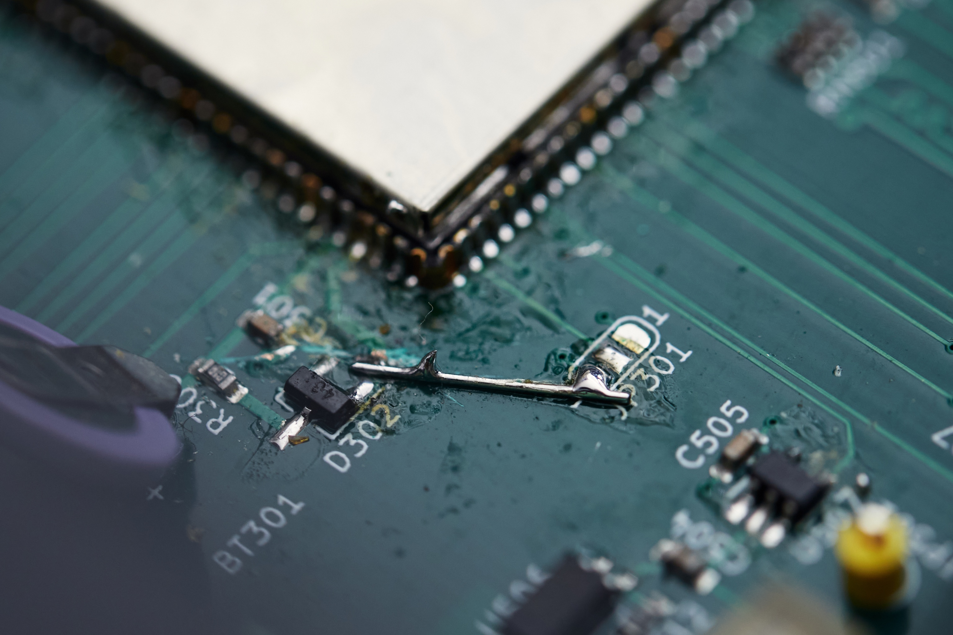
Anyways, switching the charger to use the system’s +3V3 rail (which has the benefit of a nice continuous power plane) instead (off a now unused test point for the “power key” input) solved that issue.
Though the battery footprint is still backwards. Oops. (I also didn’t notice this until after I soldered the battery and measured -2.3V at the \(V_{\text{bat}}\) input of the SoM. Double oops. It also overcharges the battery slightly, to about 3.15V. That’s like 2.5 oops-es total.)
Anyhow, all that isn’t going to be a problem in the next rev, as I’ll be changing the entire power arrangement yet again to simplify things. The SoM can supposedly provide up to 1A of +3V3 power, which should be more than sufficient for anything I need: as it stands, the whole system draws roughly 50mA at 20V, so clearly nowhere near an amp off the +3V3 rail.7
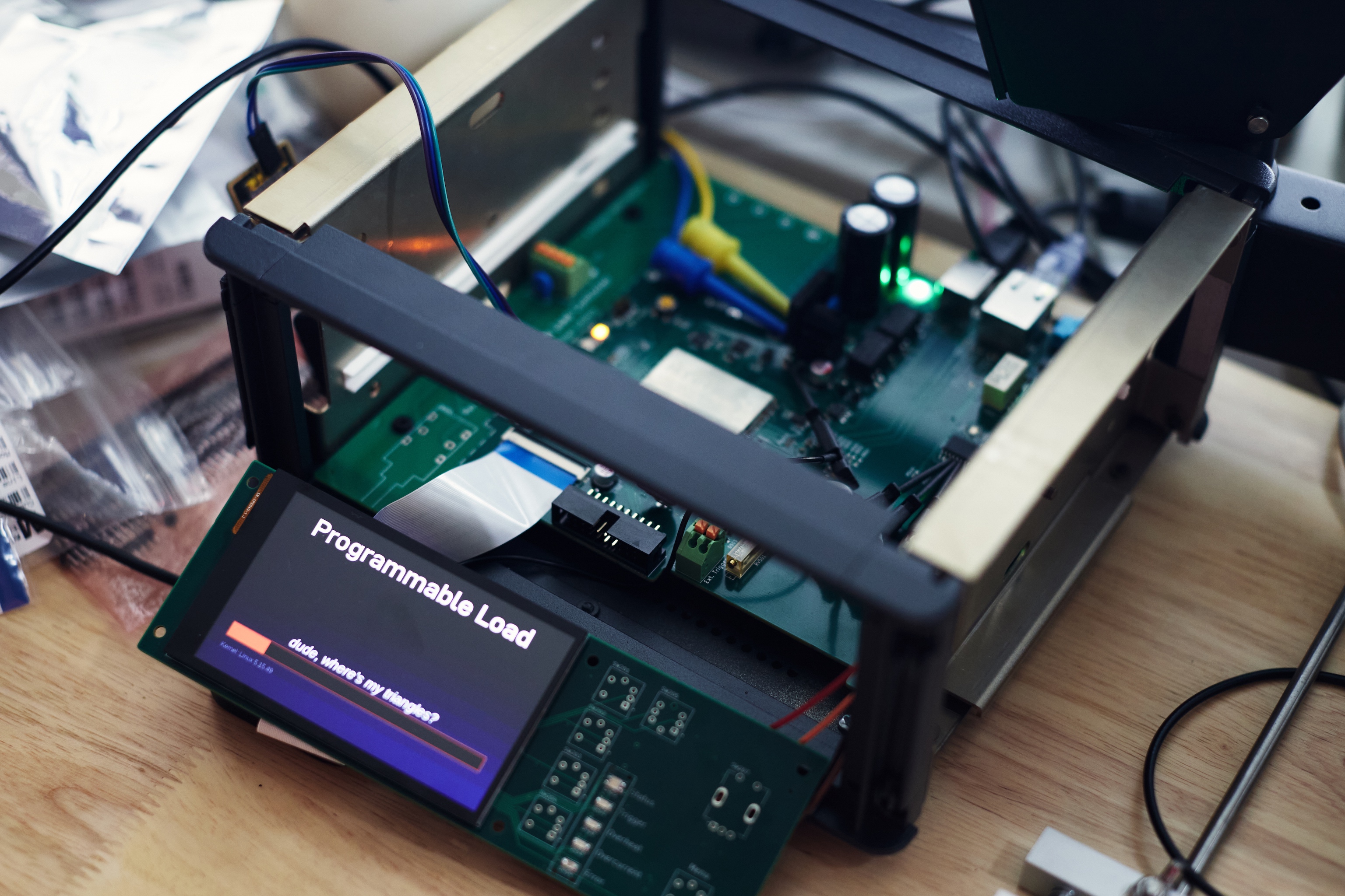
Front Panel
The most immediately visible change to the hardware comes on the front panel. As mentioned above, the display is now a 3.97” 480x800 24-bit RGB display driven by a framebuffer in the STM32MP151. I’ve also opted for the version with a capacitive touch screen, though we’ll see how much I make use of that.
I chose this display since it has a relatively high pixel density and decent contrast: nothing grinds my gears more than crappy displays, often coupled with horrendously underpowered controllers driving them.
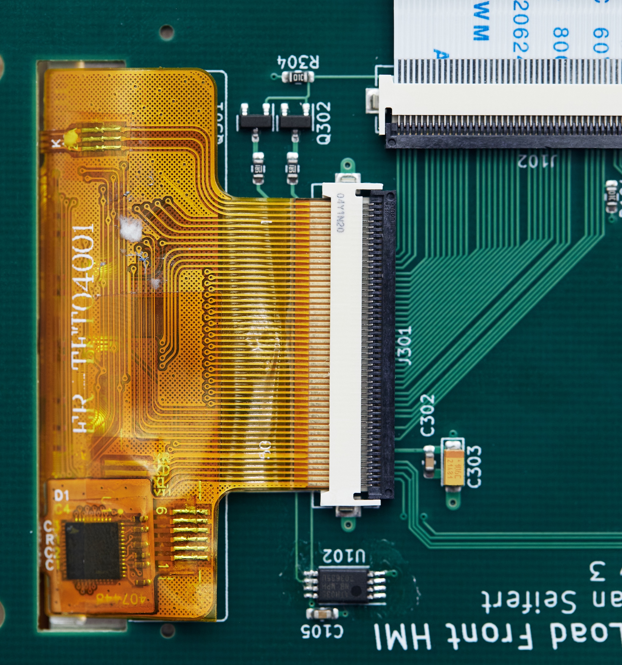
Other than extending the full width of the front panel, this board is essentially the same as the previous version. It features the same GPIO expander + LED driver setup on the I²C bus.8
With the front panel, I wasn’t as lucky as with the controller board in terms of errors: I got the pinout of the FPC connector linking it to the main board reversed. It still works, but the FPC needs to be much longer (and have a 180° twist) to connect, which is far from ideal.
Other than that, and mechanically speaking, I was actually genuinely surprised at how well everything fit together. I was rather confident in the rest of the system (since I have it modelled in FreeCAD) but I did not have 3D models of the display available, so I was making educated guesses when it came to many things, such as the size of the board cutouts and how long the display flex cutouts need to be.
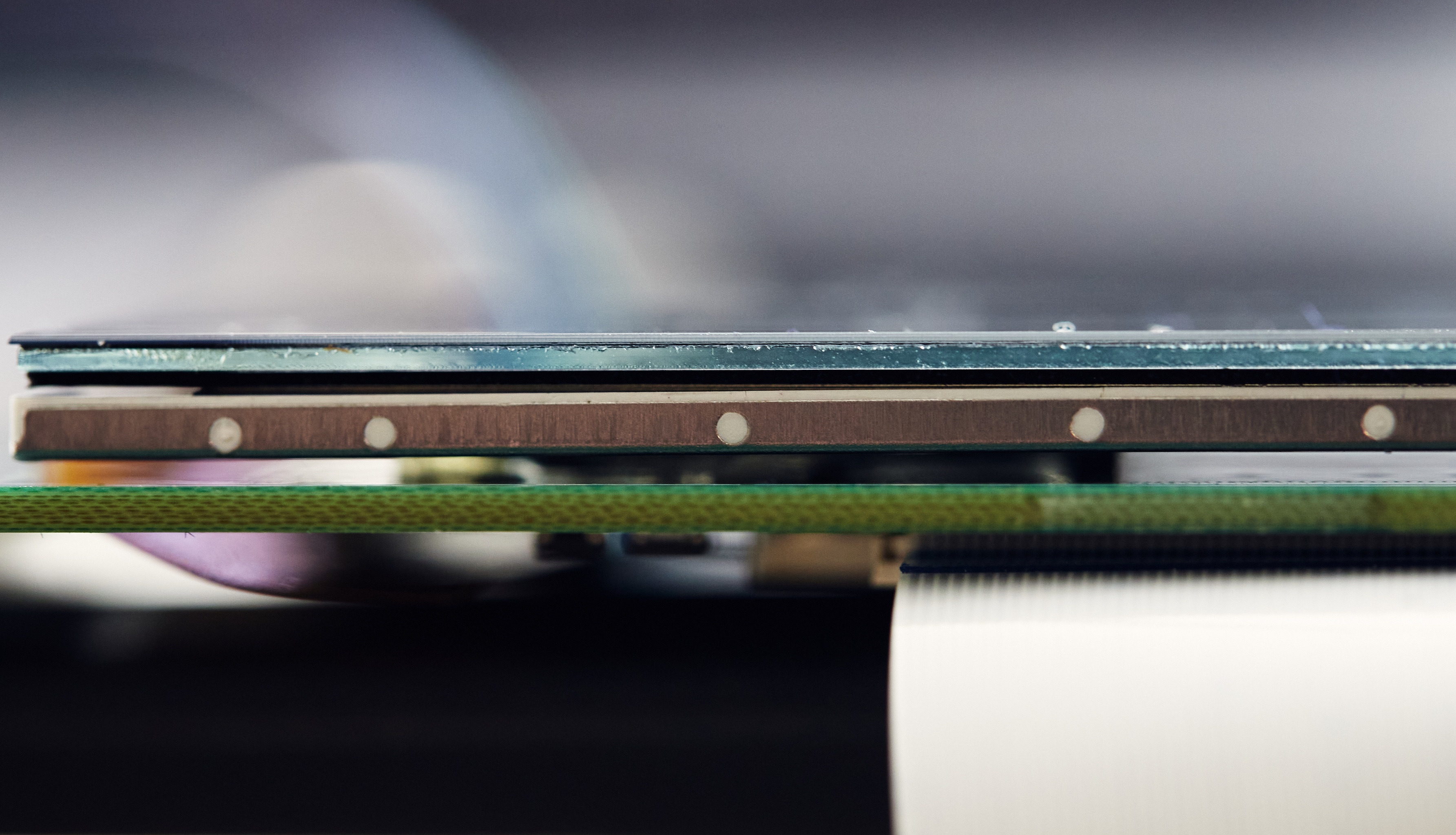
Since height is at a premium on this board (there’s 8mm of clearance between the board surface and the inside face of the front panel,) I integrated the “bare” LCD (rather than using one on an existing PCB carrier) onto the board itself. Above, you can see from top to bottom the touchscreen digitizer, the panel glass, backlight, some out-of-focus double-sided adhesive, and then finally, the PCB.
On LCD Bring-Up
I also spent way longer than I should have debugging the LCD and why I couldn’t get it working, and damn near considered giving up computers and moving to a cabin in the woods: if not only because this display is solid white when it’s powered on, but not initialized properly, rather than black, as one would expect.
Thankfully, getting the display working came down to two different things screwing me over at once. Two things I seemingly have to constantly re-learn:
Logic captures are worth their weight in gold
(What’s the exchange rate from bytes to grams of gold, anyhow?)
I started by getting my driver to read out a few device ID and panel ID registers, for matching to the correct initialization command sequences. However, no matter what I did, I could never get any actual valid data back. I assumed the display was broken, or I screwed up somewhere in my hardware and fired off an email to the vendor.9
Only after I gave up, made a trip to the local kushery, and started contemplating where my cabin would go, did I attach my logic analyzer to the other SPI bus on the board (I didn’t think to add test points on the front panel board: so I guess that’s a good thing to start doing, especially if you don’t think you need them) expecting to see nice pristine SPI packets.
I’ll let you spot the problem…
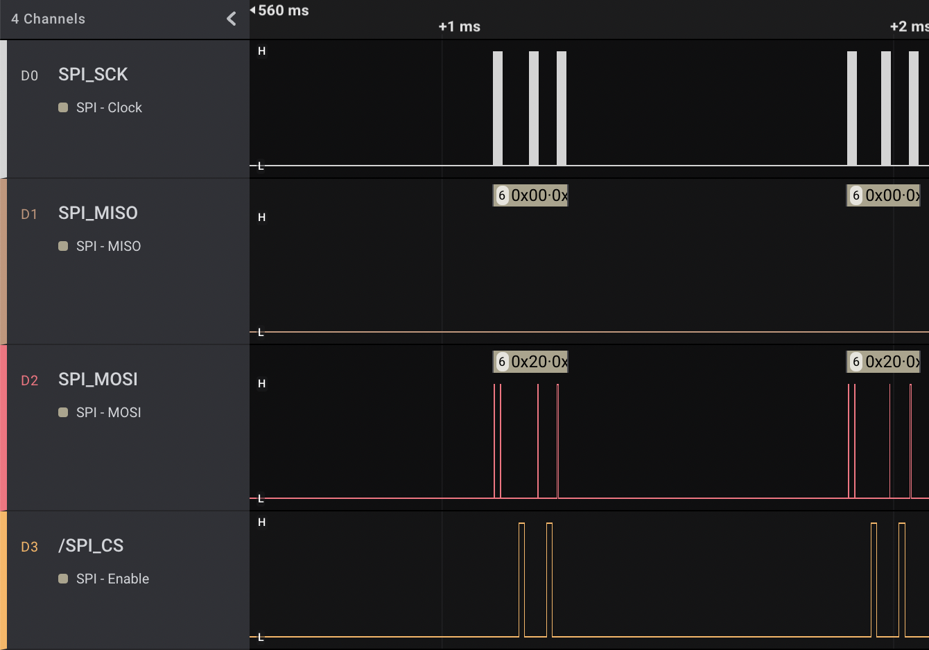
The chip selects are low when they should be… but also at plenty of other times: something is horribly wrong with the SPI driver in the 5.15.y kernel series with the chip select management. I got around this by manually setting the state of the CS line. At some point, I’ll have to debug this issue further. (There’s a good chance there’s a driver changes ST made to the SPI driver that haven’t landed upstream.)
Go figure. If I were an SPI peripheral, I’d probably not be super happy about this either. There were likely additional glitches introduced on some or all of the signals by an analog switch, which served to multiplex a single onboard SPI into separate lines for the front panel, and CAN controller for signal integrity reasons.
I’d never have gotten past this if I didn’t go and hook up my logic analyzer. And I didn’t even have to break out the big guns for this one!
Datasheets lie. Often.
The LCD I used is based on the NT35510 controller. The only datasheet I could find is version 0.00 “preliminary,” and is missing much information. There’s also an “application note” that contains most of the information needed. Both of these were adamant the display would show RGB data without initialization.
Which turned out to be a complete and utter lie. You absolutely have to configure about 37 billion different registers before the display does anything, and even then, it’s horribly picky about everything.
And when they don’t lie, they probably just suck
Once I was able to establish communication with the display, I could have it read individual frames into the memory, then scan them out under its own clock, but not receive an external clock directly. So clearly my video timings were off.
There are a few mentions here and there of how the controller calculates timings and some minor constraints like minimum lengths of the sum of the horizontal/vertical porches. But no outright display mode mentions, and clearly the “logical” display mode I put together based on online calculators and other displays in the Linux panel-simple.c driver didn’t work.
The only mention of any sort of timing intervals in in registers that the datasheet is adamant aren’t used when being clocked externally. (Those turned out to be hard requirements even when you use an external pixel clock if you’re wondering.)
Anyways, if you’re coming here in search of a video timing mode for the ER-TFT040-1, here’s what worked for me:
- Pixel clock: 25MHz
- Horizontal active display: 480 pixels
- Front porch: 10 clocks
- HSync duration: 10 clocks
- Back porch: 15 clocks
- Vertical active display: 800 pixels
- Front porch: 28 lines
- VSync duration: 3 lines
- Back porch: 28 lines
If you’re using the display mounted horizontally like I am, you’ll need to rotate it in software. The display scans from top to bottom (the side with the LCD controller flex) by default. The display is incredibly picky about the length of the vertical front/back porches. (These come from the documentation for the DPFRCTR1 command.)
What’s Next?
Glad you asked! Another board revision, of course. (Maybe not immediately, but it’ll be nice to correct some of these annoying issues.)
I have enough hardware working now to start developing some of the core software to drive everything. For now, I’ve been focusing on the Linux side of things running on the A7 core, but I’ll have to write firmware for the M4 core as well – likely a port of what I already wrote for the previous hardware, so I can use its thermal management and basic control loop functionality.
The updated boards are available on GitHub as usual if you’re so inclined to take a look, though there’s already that aforementioned next revision in the works 😉
This post was originally going to also contain a bunch of info about the custom Linux distro I created to support this project, and some semi-successful efforts in porting FreeBSD, but it looks like the hardware changes were a bit more numerous than I remembered, and this post already reading more like the next Great American novel. I’m saving those topics for a follow-up to this one, which I hopefully get out the door sooner than later.
Aside: PCB Assembly
Somewhat related, this was my first time using the JLCPCB SMD assembly service, and I gotta say, I’m pretty impressed. I’ve used them for boards for quite a while (the quality has always been decent, and the price more than good) so figured I’d give that a squiz.
Component prices are really quite reasonable, especially for the jelly-bean parts like capacitors, resistors and connectors. Many of these parts have no extra charge, but most ICs, and many more niche components incur a $3 one-time labor charge.
Exporting the required pick-and-place files from KiCAD is relatively straightforward as well, although any inevitable screw-ups will get rectified by one of their engineers based on silkscreen markings.
One downside to this service is you’re limited to green PCBs. I guess at the end of the day it doesn’t really matter, since they’re going into a pretty enclosure anyways, and I think it’s probably a fair trade-off to save myself hours of soldering flimsy little 0603 passives.
This is the third revision, and the third time’s the charm, or something. ↩
I originally planned to use this devboard to prototype an expanded, multi-channel WS2812 LED strip controller, to complement the earlier two channel controllers I designed for my networked lighting effect system. And then I graduated from university, got a job, moved across the country… and completely forgot about this board, and my grand plans. Thankfully, I found it while re-organizing my pile of devkits in my lab, as it came in really handy to evaluate whether the chip would be suitable for use with the programmable load. ↩
This is solely because I insist, for no good reason, on designing and building my own reflow controller. For which parts totally haven’t been sitting in my lab for three months… ↩
Depending on how much you’ve worked with hardware, you’ll read this as either an insult or a compliment. ↩
Using a transformer ends up being a bit more expensive and taking a fair bit more space over an AC/DC switcher, but I figured it was a worthwhile tradeoff for the significantly decreased noise and better isolation. Plus it means I get to include a voltage selector switch, like all “real” test gear 🫠 ↩
Yet I don’t have any concrete data on current consumption here. I thought about adding current sense resistors (or other power supervision type stuff) on the supplies, but it didn’t seem worth the added cost and complexity. ↩
However, I do have some plans to change that, so I can eschew the LCD initialization from the A7 side, and replace the IO expander + LED driver with a single microcontroller. But for now, that’ll do. ↩
To their credit, they got back to me within a day, told me my supposed hardware screw-ups weren’t screw-ups at all, and that my problems were probably software – I just needed to “find a friend to help you to check the software again” (To nobody’s surprise, it was a software problem.) ↩